- +61 1300 BUY PCB (1300 289 722)
- +61 3 9111 1887
For quick, professional and Friendly PCB manufacturing and PCB assembly you can rely on, talk to QualiEco Circuits
Technical Articles
Technical Articles
Bow & Twist (Part II) – Minimise the Non-Conformance by Improving PCB Design, Production & Assembly Processes
We learned the basics of Bow and Twist and its calculation methods in Part I of this technical guide. In this guide, let us understand how to improve PCB design, production and assembly processes so that bow and twist can be avoided or its effects are minimised.
Following are the PCB design, manufacturing and assembly practices that a designer should adopt:
How to Improve the PCB Design Process?
Copper Balance
Designing a circuit board with a symmetrical copper distribution is extremely important to minimise the effects of a Bow and Twist on the final PCB. Because copper has a high coefficient of thermal expansion, high density copper expands towards the area of least resistance at greater force than a low density copper area.
The HASL (Hot Air Solder Level) process in PCB manufacturing or Reflow process in PCB assembly causes thermal load in the circuit board. During these processes, the laminate is exposed to temperatures above the glass transition (Tg) temperature. Even though the epoxy will try to expand in all directions, mechanical devices such as Component Holes (PTH) and Vias act as reinforcements and work to restrict the even expansion, which results into some degree of wave, sag or bow. If the PCB is designed with the correct symmetry, such increase in deformation normally falls within an allowable Bow and Twist limit set by IPC. However, if the PCB design consists of asymmetrical copper distribution, the thermal load generated within the copper area will eventually cause warpage in the PCB and may surpass its IPC limit.
Following are the rules of thumb that a designer should follow to minimise the warpage:
-
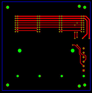
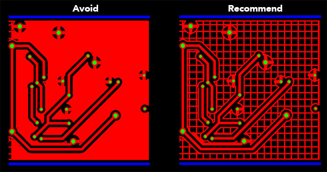
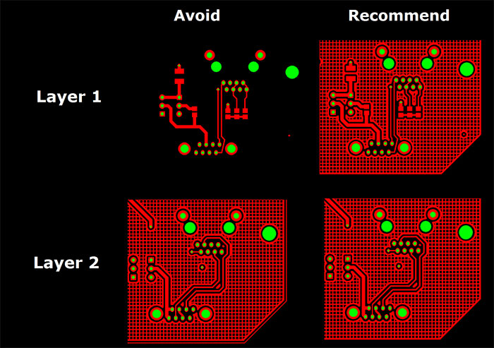
To avoid “copper nests” created in your design, ensure that your conductor traces are distributed as uniformly as possible across the board. This not only should apply within each layer but also across any axis of symmetry between two or more layers.
-
Large copper area in the design should be in a grid form instead of solid copper provided there are no sensitive high frequency conductor traces present. Having a grid helps to minimise the effect of a Bow and Twist to a great extent, especially in a single layer PCB.
-
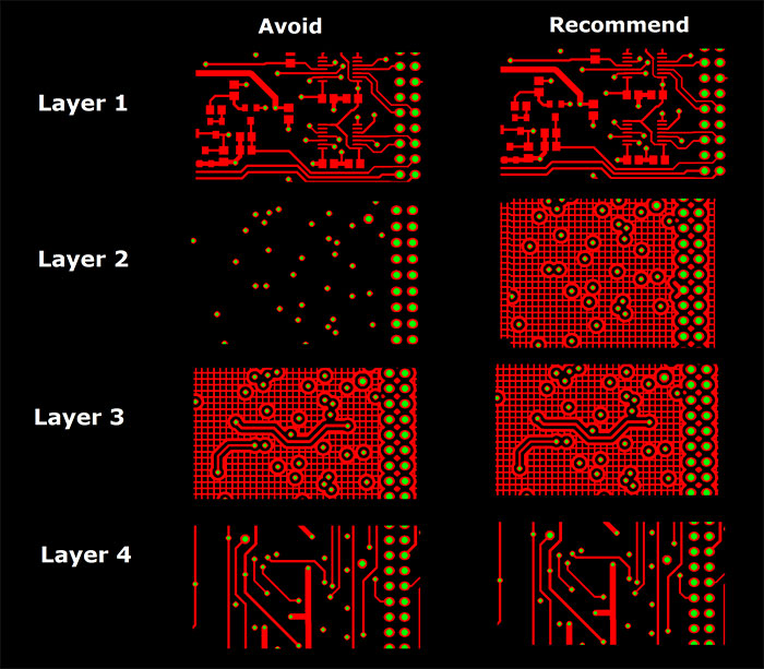
If large copper areas are needed in a design, care must be taken to ensure they are counterbalanced with a copper filling in the layer symmetrically opposite. Let us understand this principle with the help of a hypothetical copper balance bar, layer construction and copper weight calculation.
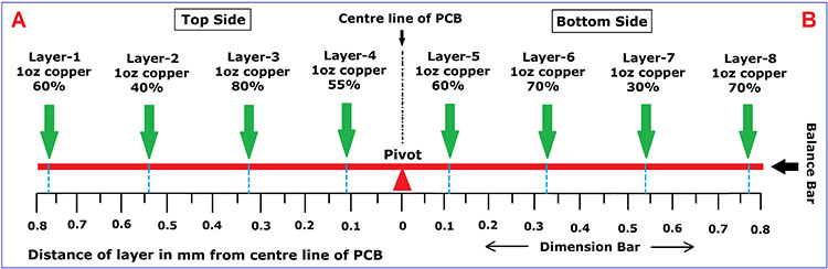
| Copper Balance | A = 3.51 (1.62+0.76+0.92+0.21) |
Layer-1 = 60 x 0.035 x 0.77 = 1.62 |
| Layer-2 = 40 x 0.035 x 0.54 = 0.76 | ||
| Layer-3 = 80 x 0.035 x 0.33 = 0.92 | ||
| Layer-4 = 55 x 0.035 x 0.11 = 0.21 | ||
| B = 3.53 (0.23+0.81+0.57+1.89) |
Layer-5 = 60 x 0.035 x 0.11 = 0.23 | |
| Layer-6 = 70 x 0.035 x 0.33 = 0.81 | ||
| Layer-7 = 30 x 0.035 x 0.54 = 0.57 | ||
| Layer-8 = 70 x 0.035 x 0.77 = 1.89 |
Since the concept of copper balance is now clear, here are couple of examples (2 & 4 layer PCB) how the design can be improved –
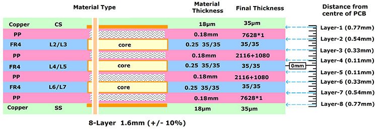
Layer Structure Symmetry
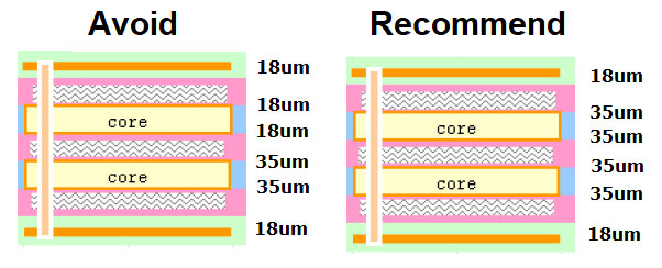
A Multilayer PCB should be designed using symmetrical stack up (copper weight and core/prepreg thickness) unless there is a restriction of an impedance control.
Mixing of Materials
Mixing different types of laminates causes deformation and should be avoided e.g. high frequency laminate with standard FR-4 are used in some designs to control impedance values.
Quantity and Location of Break off Holes (Mouse Bites)
The least focused area in a PCB design is the final panelisation of individual circuits for SMT assembly. An effective and smart layout of the tooling strip and break off tab size/location helps reduce the Bow and Twist to a great extent. The technical team at QualiEco has expertise to panelise individual circuits effectively to ensure adequate strength to the panel as well as lowering the possibility of warpage.
How to Improve the PCB Manufacturing Processes?
- For multilayer PCBs, mixing of a core and a prepreg from different laminate manufacturers should be avoided.
- PCBs having troubled records of Bow and Twist can be baked before shipping for 3-4 hours at 150 degrees and then letting it cool down naturally. This will reduce the mechanical stress generated during the PCB manufacturing process.
- Circuit boards consisting of blind and buried vias are subject to more Bows and Twists. Therefore, extra care should be taken during manufacturing.
- Good storage condition is extremely important to preserve the laminate flatness not only inside the incoming storage area but also while stacking PCB panels during production.
How to Improve the PCB Assembly Processes?
- Heavy thermal shocks should be avoided by selecting appropriate soldering profile
- The conveyor should be wide enough to accommodate the complete width of the circuit board. In the absence of this, the Bow and Twist may be generated in a PCB if the components are heavy in weight.
- Ensure adequate support to a PCB panel during soldering process
PCB Design Tips
When designing a PCB, try to limit the amount of draws you use. Draws use a lot of memory and slow the programming time. Use a flash for pads instead.
More tips...
Contract Assembly
We are one-stop solution provider for all your contract assembly requirements. We have the capability and resources to provide PCB assemblies, as well as cable and harness assemblies.


What our customers say?
QualiEco Circuits Limited is an excellent supplier to us! We appreciate the quality of service and support that we receive from QualiEco Circuits. They always deliver what is promised
For printed circuit boards (PCBs) or PCB assembly you can count on. Talk to the friendly and experienced team at QualiEco Circuits, Australia.