- +61 1300 BUY PCB (1300 289 722)
- +61 3 9111 1887
For quick, professional and Friendly PCB manufacturing and PCB assembly you can rely on, talk to QualiEco Circuits
Technical Articles
Technical Articles
How to read and understand QualiEco’s technical capability statement
Imagine a situation that you have designed a complex circuit board and released to QualiEco for quoting. Instead of receiving quote, you are advised to make few changes in design to suit our manufacturing capability. How do you feel when these changes take days to implement and disturb your project planning? Extremely frustrating and it’s not hard to guess.
Wouldn’t it be convenient if you know how to check our capability statement and use that information in your designing process?
Here are some tips:
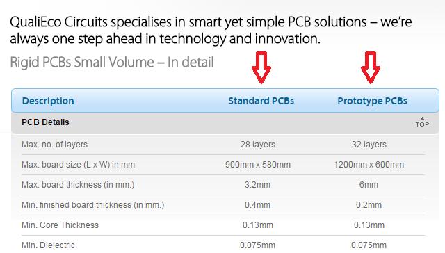
1. QualiEco has separate capability statement for prototype and production. Please ask us if you are not sure which one to refer. It is possible to manufacture small volume PCBs with tighter tolerances so if you require PCBs in small numbers, you may choose our tightest capability.
2. There are 3 BASIC technical limitations you must know before you start designing PCB -
(a) Etching limitation (i.e. minimum track width/spacing)
For 1oz standard finish copper thickness PCBs, 5-6mil (i.e. 0.127-0.152mm) is the minimum track width and spacing requirement for most manufacturers. With special attention, 3.5-4mil (i.e. 0.089-0.102mm) can be achieved on small to medium volume production. If your design requires thicker copper then minimum track width/spacing can increase up to 12 or 13mils depending on how thick copper you require.
(b) Hole size limitation
Most manufacturers accept finish hole sizes from 0.3mm and higher as standard. Some manufacturers charge extra for 0.25mm finish holes (standard for QualiEco Circuits). QualiEco can also accept 0.2mm finish holes by paying extra. In few exceptional cases, 0.15mm finish hole size can also be acceptable using mechanical drilling process. Any less than 0.15mm can only be possible by laser drilling process, which is quite expensive.

(c) Bonding & Drilling limitation - for multilayer PCBs only
The most important criterion to keep in mind while designing multi-layer PCB is the gap between edge of the hole and nearest copper area (track/pad/pour) in inner layers. For multi-layer PCBs, drilling is performed after bonding so this criterion is extremely critical for all PCB manufacturers.

It is very important to know whether plating tolerance has been added while mentioning minimum isolation in any technical capability statement. Most manufacturers including QualiEco need to add approximately 0.1mm plating tolerance for via holes. Some manufacturers display minimum isolation sizes without adding plating tolerance while some do add them. Unfortunately, there is no specific guideline for displaying this criterion.
3. Another important factor to consider in your design is the minimum copper and solder mask pad size around holes.
(a) Copper pad size
Most manufacturers define copper pads around holes as “annular ring”. There is a minimum annular ring size you need to maintain everywhere in the design.


(b) Solder mask pad size
Solder mask is nothing but an opening to prevent solder bridges between adjacent pads and traces during soldering process. Most manufacturers define such opening as “mask opening”.


PCB Design Tips
When designing a PCB, try to limit the amount of draws you use. Draws use a lot of memory and slow the programming time. Use a flash for pads instead.
More tips...
Contract Assembly
We are one-stop solution provider for all your contract assembly requirements. We have the capability and resources to provide PCB assemblies, as well as cable and harness assemblies.


What our customers say?
QualiEco Circuits Limited is an excellent supplier to us! We appreciate the quality of service and support that we receive from QualiEco Circuits. They always deliver what is promised
For printed circuit boards (PCBs) or PCB assembly you can count on. Talk to the friendly and experienced team at QualiEco Circuits, Australia.